Advanced Electromagnetic Research & Antenna Laboratory
State-of-the-art research facility for wireless communication, antenna engineering, and RF system development.
About Parul University
Situated at the heart of the cultural capital of Gujarat, Vadodara, Parul University is a testament to the fusion of rich cultural heritage history and the contemporary 21st century. Since its inception in 1993 to its recognition as an University in 2015, Parul University has emerged as one of the largest and leading academic institutions.
The university is a rich blend of 21 faculties and 38 institutes offering a wide range of diploma, graduate, and postgraduate degree programs in various academic disciplines.
About AERAL
The Advanced Electromagnetic Research and Antenna Laboratory (AERAL) is a state-of-the-art research facility established in the Micro and Nano Research and Department Center to support advanced exploration in wireless communication, antenna engineering, and RF system development. The laboratory enables researchers to innovate across a wide range of electromagnetic applications, including conventional and planar antennas, RF and microwave systems, metamaterials, fractal structures, implantable antennas, energy harvesting devices, and bio-electromagnetic studies.
AERAL provides an end-to-end platform for simulation, high-precision measurement, and performance evaluation of antennas and RF devices. The lab supports comprehensive testing capabilities, including S-parameter measurement, 2D and 3D radiation pattern analysis, gain measurement, and axial ratio measurement, ensuring accurate validation of advanced electromagnetic designs.
Our Facilities

CST Microwave Studio (Software)
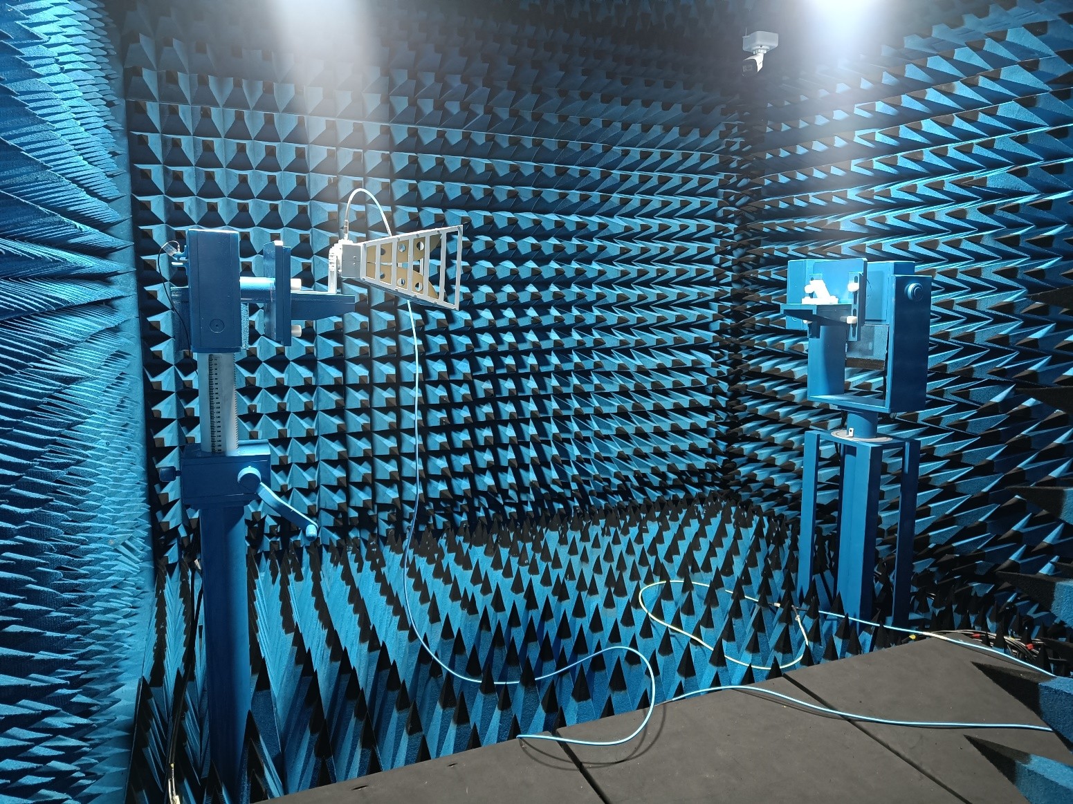
RF Anechoic Chamber
The RF Anechoic Chamber provides a controlled, reflection-free environment essential for accurate antenna and RF measurements. Lined with high-performance electromagnetic absorbers, the chamber eliminates unwanted reflections and external interference, ensuring reliable testing up to 18 GHz. Equipped with automated multi-axis positioners, reference antennas, and integrated control software, the chamber supports 2D/3D radiation pattern measurement, gain estimation, axial ratio evaluation, and S-parameter characterization. It serves as a critical facility for validating antenna prototypes, metamaterial structures, and RF systems.
The measurement facility is used to test antennas in terms of port performance and radiation performance. The port performance is measured using an Anritsu VNA to determine S-parameters and VSWR up to 20 GHz. The radiation performance is measured in this far-field type chamber, where RF absorbing material on the walls and doors simulates a free-space environment. The facility characterizes E- and H-Plane patterns and Gain for planar/non-planar low-profile antennas in the frequency range of 0.5 GHz to 18 GHz with a maximum far-field of 1.5 meters.
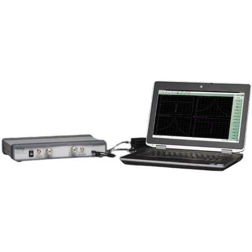
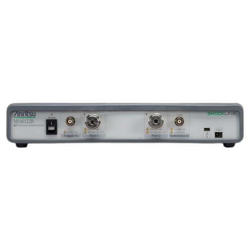
Vector Network Analyzer (1 MHz – 20 GHz)
The ShockLine™ MS46122B series consists of three PC-controlled, compact vector network analyzers (VNAs) with frequency ranges from 1 MHz to 20 Ghz. The series benefits from patented shockline VNA-on-chip technology that simplifies the internal VNA architecture at high frequencies, reduces instrument cost, and enhances accuracy and measurement repeatability. All the members of the ShockLine MS46122B series are low-cost, full-reversing, 2-port VNAs aimed at RF and microwave applications within manufacturing, engineering, and education organizations.
The VNAs has 130 microseconds per point sweep speed and better than 100 dB dynamic range, making them suitable for a variety of device test applications including measuring passive 5G mmWave components. This VNA is packaged in a very compact and portable 1U chassis, are externally controlled via USB from a user-supplied PC, and powered using an external power supply brick.
The ShockLine MS46122B VNA series are controlled using the same graphical user interface (GUI) and driver software as the rest of the ShockLine family of VNAs. The series does not have any on-board memory, which simplifies their use in secure applications. The combination of lower cost, small size, and good performance make the ShockLine MS46122B VNA series ideal for passive device test applications where portability and space efficiency are key.
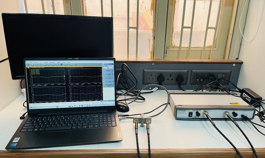
X-Band Dielectric Measurement (8–12 GHz)
Our laboratory offers dielectric characterization in the X-band frequency range (8–12 GHz) using a Vector Network Analyzer (VNA) integrated with a rectangular waveguide RF adapter. This facility enables accurate extraction of complex permittivity parameters over the X-band. During measurement, the material under test (MUT) is precisely inserted into the X-band waveguide section, and the reflection (S11) and transmission (S21) parameters are recorded after proper two-port calibration.
The measured data are processed to determine the material’s dielectric constant (ε′), dielectric loss (ε″), and loss tangent (tan δ) across the specified frequency range. For accurate and repeatable results, the sample dimensions must strictly conform to the internal dimensions of the X-band waveguide, ensuring complete filling of the cross-section and eliminating air gaps. Proper sample thickness is maintained to minimize measurement errors and unwanted mode excitation.
Key Features:
- Frequency range: X-band (8–12 GHz)
- Measurement using rectangular waveguide RF adapter
- Sample size as per waveguide cross-section dimensions
- Extraction of ε′, ε″, and tan δ
- High accuracy for solid and slab-type materials
- Suitable for research and industrial material evaluation
Sample Requirements
- •Planar/Non-planar, Active/Passive antennas can be characterized.
- •Antennas heavier than 5Kgs can't be tested. The far-field is limited to 1.5 meters only.